
By MICHAEL FLITTON
ASML is the dominant supplier of photolithography tools for semiconductor manufacturers.
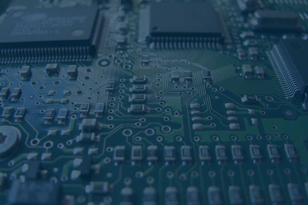
Photolithography is the process of printing with light. In semiconductors it is the process whereby a light source is used to expose circuit patterns onto a wafer via a photomask.
Photolithography has played a pivotal role in the evolution of semiconductors. It was Robert Noyce (future co-founder of Intel) at Fairchild Semiconductors in 1960 who saw the potential of the process to enable the printing of electronic circuits on flat, silicon wafers. This vision gave birth to the first integrated circuit and catalysed the race to ever smaller geometries in chip design.
As transistor scale approaches the atomic level, the next limiting factor for the continuation of Moore’s Law1 is the wavelength of light. The shorter the wavelength, the smaller the scale in which a circuit can be printed. A radical reengineering of the lithography process is required. For the last 20 years ASML has been working on just such a radical solution. EUV or Extreme Ultraviolet lithography drops the wavelength of light from 193nm to 13.5nm enabling the extension of Moore’s Law through 2025. The payoff for this commitment of capital, and shouldering of risk, is 100% market share prospectively. We observe a high moat around the business supported by a technology ecosystem which peers will find difficult to emulate.
Within the Global Leaders portfolio ASML joins TSMC and Samsung from the semiconductor supply chain. As a result, this industry is better represented than most, which merits explanation. Demand in semiconductors is one of the few structural trends we can observe with confidence over a 10-year time horizon. All three businesses also demonstrate similar properties we find attractive: a picks and shovels exposure to demand and accelerating barriers to entry from know-how and scale.